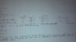
Activity 2.2.1
At this point you have the capability to apply the theorems and laws of Boolean algebra to simplify logic expressions to produce simpler and more cost effective digital logic circuits. You may have also realized that simplifying a logic expression using Boolean algebra, though not terribly complicated, is not always the most straightforward process. There isn’t always a clear starting point for applying the various theorems and laws, nor is there a definitive end in the process.
Wouldn’t it be nice to have a process for simplifying logic expressions that was more straightforward, had a clearly defined beginning, middle, and end, and didn’t required you to memorize all of the Boolean theorems and laws? Well there is, and it is called Karnaugh mapping. Karnaugh mapping, or K-Mapping, is a graphical technique for simplifying logic expressions containing up to four variables.
In this activity you will learn how to utilize the Karnaugh mapping technique to simplify two, three, and four variable logic expressions. Additionally, logic expressions containing don’t care conditions will be simplified using the K-Mapping process.\
Conclusion
-NOT "A'" C
At this point you have the capability to apply the theorems and laws of Boolean algebra to simplify logic expressions to produce simpler and more cost effective digital logic circuits. You may have also realized that simplifying a logic expression using Boolean algebra, though not terribly complicated, is not always the most straightforward process. There isn’t always a clear starting point for applying the various theorems and laws, nor is there a definitive end in the process.
Wouldn’t it be nice to have a process for simplifying logic expressions that was more straightforward, had a clearly defined beginning, middle, and end, and didn’t required you to memorize all of the Boolean theorems and laws? Well there is, and it is called Karnaugh mapping. Karnaugh mapping, or K-Mapping, is a graphical technique for simplifying logic expressions containing up to four variables.
In this activity you will learn how to utilize the Karnaugh mapping technique to simplify two, three, and four variable logic expressions. Additionally, logic expressions containing don’t care conditions will be simplified using the K-Mapping process.\
Conclusion
- Give three advantages of using K-mapping to simplify logic expressions over Boolean algebra.
-NOT "A'" C
Activity 2.1.2
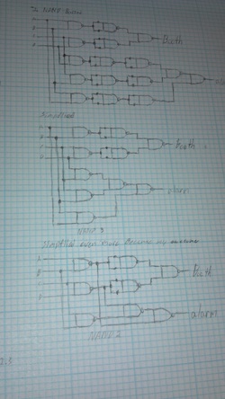
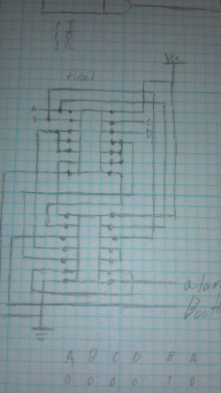
The block diagram shown below represents a voting booth monitoring system. For privacy reasons, a voting booth can only be used if the booth on either side is unoccupied. The monitoring system has four inputs and two outputs. Whenever a voting booth is occupied, the corresponding input (A, B, C, & D) is a (1). The first output, Booth, is a (1) whenever a voting booth is available. The second output, Alarm, is a (1) whenever the privacy rule is violated.
In this activity you will implement NAND only combinational logic circuits for the two outputs Booth and Alarm. These NAND only designs will be compared with the original AOI implementations in terms of efficiency and gate/IC utilization. In a future activity, these NAND only designs will be compared to the circuits implemented using only NOR gates.
Conclusion
1. For your AOI implementations, how many ICs (i.e., 74LS04, 74LS08, and 74LS32 chips) were required to implement your circuits? Note: You’re not just counting the number of gates used, but rather, the number of IC, in whole or part, that were required.
-4
2. For your NAND implementations, how many ICs (i.e., 74LS00 chips) were required to implement your circuits? Again, we are counting ICs, not gates.
-3
3. In terms of hardware efficiency, how does the NAND implementation compare to the AOI implementation?
-NAND chips can make AOI logic
4. NAND gates are available with three inputs (74LS10) and four inputs (74LS20). Could either of these chips have been used for this design? If so, how would it have affected the efficiency of the design?
- pending on how the circuit is laid out
Activity 2.2.3
In this activity you will revisit the voting booth monitoring system introduced in Activity 2.2.3 NAND Logic Design. Specifically, you will be implementing the NOR only combinational logic circuits for the two outputs Booth and Alarm. In terms of efficiency and gate/IC utilization, these NOR only designs will be compared with the previously designed AOI and NAND implementations.
1. For your NOR implementations, how many ICs (i.e., 74LS02 chips) were required to implement your circuits? Again, we are counting ICs, not gates.
-3
2. In terms of hardware efficiency, how does the NOR implementation compare to the AOI implementation (Refer to Activity 2.2.3 NAND Logic Design)?
-3 for NOR and 4 for AOI
3. In terms of hardware efficiency, how does the NOR implementation compare to the NAND implementation in Activity 2.2.3 NAND Logic Design?
- The same
4. NOR gates are available with three inputs (74LS27). Could this chip have been used for this design? If so, how would it have affected the efficiency of the design?-you could put in 1 chip
